Other Technology | September 27, 2023

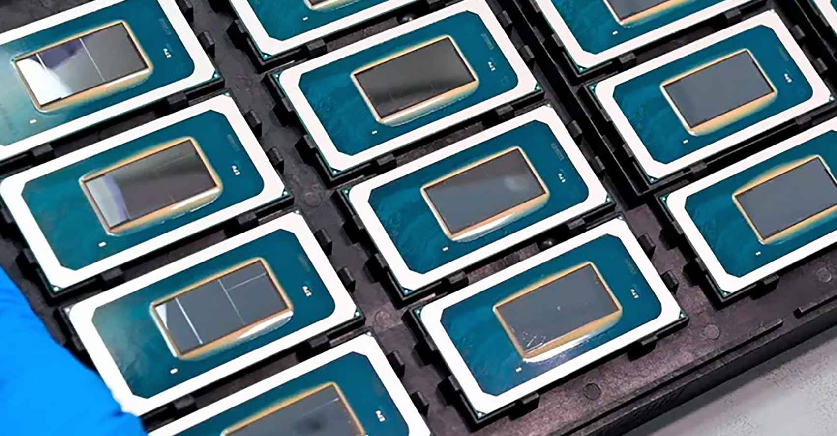
Just a week after the release of Thunderbolt 5, Intel has been eagerly awaiting this day after months of teasing that this chip will be a game-changer for the company and the industry. The Meteor Lake chip will be launched on December 14th and will become part of those ‘heterogeneous’ chips that are now common in mobile devices, tablets, and laptops.
Intel claims that it will release the most energy-efficient chip ever made by the company to double graphics performance and handle tasks independently in what it calls the ‘low-power island’ or minimal power consumption space. In fact, this chip will be embedded in Microsoft’s Windows.
In this way, the company joins AMD and Qualcomm, which have released processors where silicon components are “printed” in different sizes together; in other words, the CPU and GPU are almost “unified,” whereas these components are usually separate. So, you could almost say that Intel is a “newcomer” in this regard, albeit with all the experience of being a leader in its field.
Technically, the design of this new chip is not based entirely on Intel’s latest technology, Intel 4, as the graphics are based on TSMC’s 5nm process, and the I/O and new ‘SoC Tile’ on TMSC N6. However, manufacturers can customize this chip to maximize performance according to their product needs.
To make this chip the most efficient ever released by Intel, each Meteor Lake chip will have one of these ‘low-power islands,’ which can handle all processes independently. An important detail of this new chip is that it includes an AI processor that can be monitored from the Windows Task Manager to check its performance.
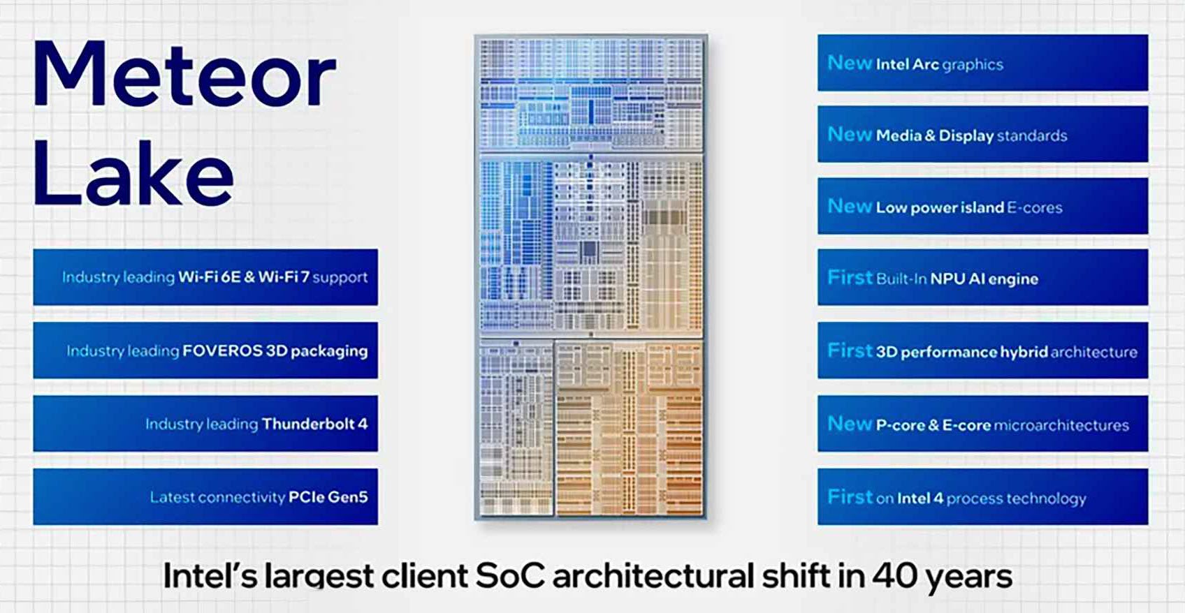
Another advantage is that the nodes responsible for ‘media’ are separate from those used for graphics, so video encoding and decoding occur without interfering with the graphics side. In addition to support for AV1 video, native HDMI 2.1, DisplayPort, and HDR 8K video, there’s another layer for Bluetooth 5.4 and WiFi 7; the latter with transfer speeds of up to 5.76 Gbps.
While these tasks for ‘graphics’ are separate from the GPU, it doesn’t mean it’s just a bystander. Intel claims that Meteor Lake can add its Intel Arc graphics. The ‘Xe LPG’ GPU offers up to twice the performance per watt of the Xe LP, which, in turn, doubles the wattage performance of the previous 11th Gen Intel UHD chip that was integrated into their processors. For gaming, Intel also includes XeSS, similar to NVIDIA’s DLSS and AMD’s FSR (which provides a significant FPS boost to games).
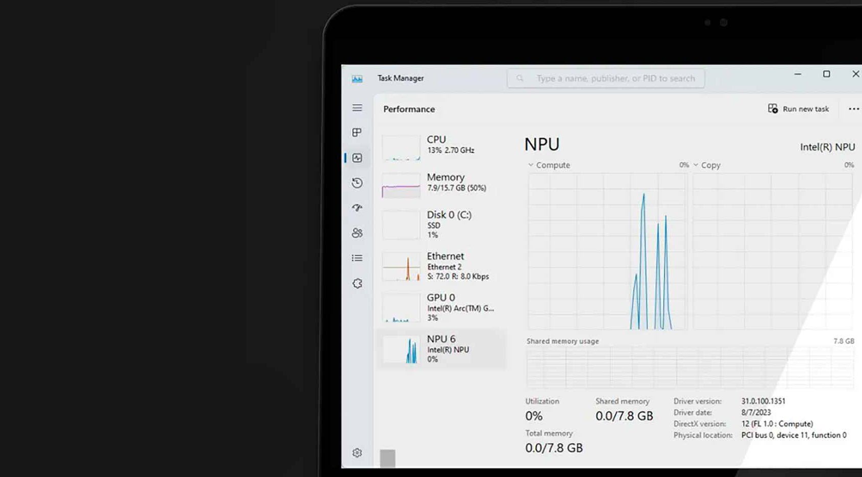
As for its AI chip, or NPU, it won’t be able to replace the chips in servers that handle generative AI, but there will be options: the NPU can handle the operation of an image generator like Stable Diffusion or be faster and more efficient when using the GPU and NPU together.
After all the technical details, according to The Verge, it’s easier to understand the importance of Meteor Lake with Intel’s investment: $3.5 billion in its facilities in New Mexico and $7 billion in Penang, Malaysia over the next 10 years.